Self-assembly mechanism and dynamics in a continuum medium
We aim to develop fundamental understanding of the self-assembly mechanism and systematic approaches to tune the process.
Self-assembly on material surfaces
Experimental evidence has accumulated in the recent decade that nanoscale patterns can self-assemble on solid surfaces. A two-component monolayer grown on a solid surface may separate into distinct phases. Sometimes the phases select sizes about 10 nm, and order into an array of stripes, disks or other regular patterns. These behaviors are intriguing because they are absent in bulk phase separation. The ability of patterning nanostructures on a surface is very important for many modern technological applications, such as in microelectronics circuits and digital storage media. It also opens up the possibility of fabricating cheap, large area devices using non‑ lithographic techniques.
Why do atoms self-assemble? What sets the feature size? The answers differ for different material systems. A unifying concept, however, can be identified. For many reasons the free energy of a material system depends on its configuration (e.g., the composition of the phases and their spatial arrangement). When the configuration changes, the free energy also changes. This defines thermodynamic forces that drive the configuration change. The change is effected by mass transport processes, such as diffusion. To assemble a nanostructure, some of the forces must act over the scale comparable to the feature size, and are therefore much longer ranging than atomic bond length.
We developed a thermodynamic framework to study the remarkable phenomena. Based on our continuous phase field model, we developed the numerical technique and performed large-scale simulation of the whole process of formation and evolution of nanostructures on a solid surface. The simulation reveals remarkably rich dynamics and suggests a significant degree of experimental control in growing ordered nanoscale structures. Our work reveals how various parameters, including free energy of mixing, phase boundary energy, surface stress, average concentration, anisotropy etc, may influence the nanostructures. The model and simulation technique provides a powerful tool to conduct “numerical experiments” and investigate various behaviors associated with nanostructure evolution. We are now studying guided self-assembly, i.e. how to grow desired fine nanoscale structures by pre-patterning some coarse structures.
The following are some examples of our simulations.
 |  |  |  |
 |  |  |  |
Through a series of works, we revealed the effect of surface stress and established the theory of guided self-assembly. This work is of significant interest since surface stress acts in many systems. Our work revealed the refining effect of surface stress, which leads to nanostructures stable against annealing. We investigated material anisotropy and revealed an approach of material tuning to form various nanostructure patterns. We developed a theory of guided self-assembly with surface chemistry and strain field, which leads to a technique to create well-aligned complex nanostructures at specific locations.
Grow an extremely large pattern of phase domains without any defect by sequential activation of self-assembly
We developed this process where self-assembly operated in a small mobile region where atoms could diffuse. The mobile region was shifted gradually so that self-assembly happens sequentially. This mechanism guaranteed no defect due to its unique self-improving capability. Particularly notable, we discovered an exciting mechanism that self-assembly propagates spontaneously in a continuum medium, enabling the delivery of local order information to distance. In this process a locally self-assembled structure destabilizes its surrounding through an elastic dipole interaction, causing order replication.

Nanomechanics and nano/micro structure evolution
We study deformation and structure evolution that involve morphological, compositional and crystal symmetry changes and their coupling. Emphasis is placed on new insight into the effect of elasticity, novel energetic forces that are critical in small scale ─ such as surface stress and molecular dipoles, concurrent kinetic processes involving diffusion and mass flow, and dynamic interaction among structures of different type and length scale.
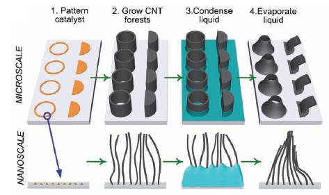
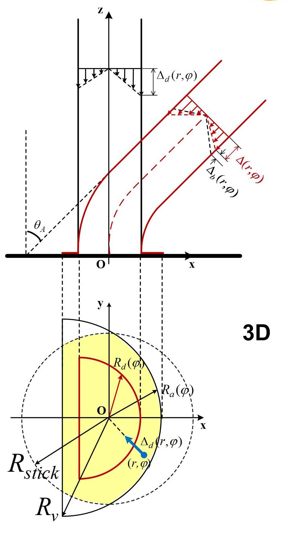
Mechanism of capillary forming of 3D nanostructures
Capillary forming enables transformation of nanoscale filaments such as patterned CNT forest microstructures into 3D freeform shapes and complex surface architectures. The method is based on condensation of liquid onto vertically aligned filaments, followed by evaporation, causing a deterministic transformation of the structures to intricate 3D shapes. We use energetic and kinetic analysis to identify the critical mechanisms of action in detail. In particular, we developed a mechanics model and revealed quantitatively that the lateral deflection and twisting can be controlled precisely by the pattern shape and the coupling strength among the filaments.
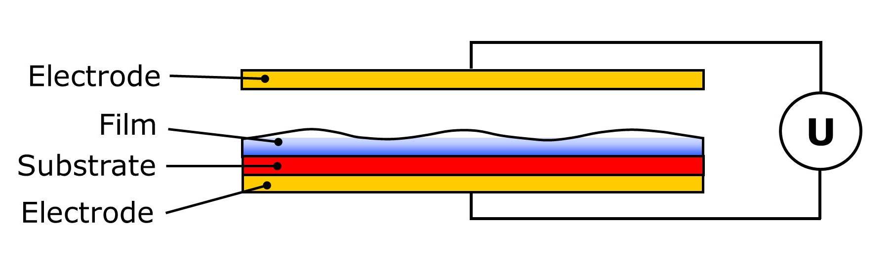
Development of novel nanofabrication technique by exploiting electric field
We heat a thin polymer film above its glass transition temperature in an electric field. After annealing the sample, we cool it and then remove the field. Periodic polymer islands rise from the initially flat film, forming a close-packed hexagonal pattern. This work reveals a mechanism to induce self-assembly by the interaction of polymer-air interface with an electric field, indicating a novel method to pattern morphological patterns in a functional polymer film. We developed a three-dimensional dynamic model that incorporates viscous flow, diffusion and dielectric mechanism to account for the behavior. Simulations revealed an approach of directing morphologies with distributed electric field and kinetic constraint. We are extending this technique to multilayer films, hierarchical nanostructures, and combined process of electric field and local heating by a laser beam.
We investigated patterning nanostructures via molecular electric dipoles and double layer charges. We developed a model for the interaction of molecular dipoles in multi-layers incorporating the dielectric property of the substrate and embedded electrodes. Simulations revealed self-alignment between layers and guided self-assembly by layer-layer interaction and electrodes. We developed knowledge to tune the size and ordering of domains, allowing patterning molecules into designed 2D/3D nanostructures.
Self-assembled polymer film
Self-assembled nanoparticle network
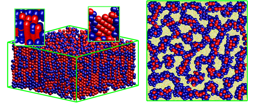
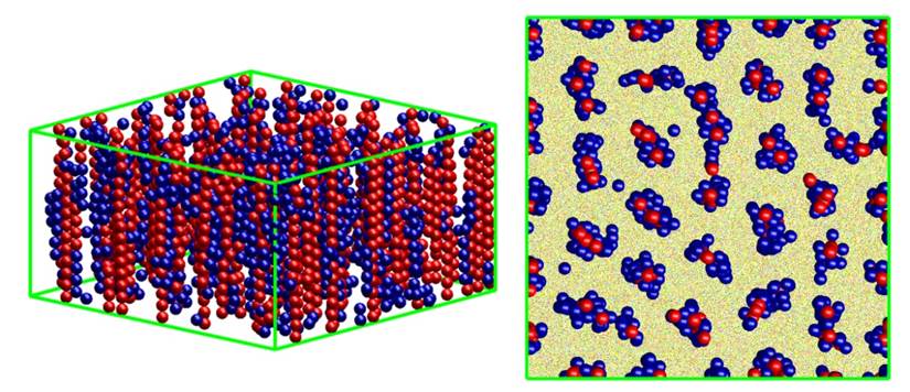
Self-assembled dipole molecules
Electrostatic printing of few-layer-graphenes
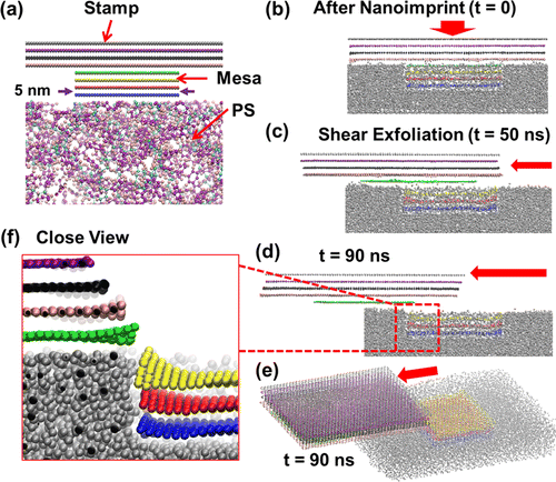
Efficient mechanical exfoliation of atomically thin layered materials (ATLMs) with accurate control over the number of printed flakes is essential for fabrication of high-performance electronic devices. We combine conductive atomic force microscopy (CAFM) and molecular dynamics (MD) simulations to study the shear and normal exfoliation mechanisms in nanoscale graphite structures. The setup also allows quantifying the effect of layer number and electric field on the dielectric constant of few-layer graphene (FLG). Our CAFM-assisted electrostatic printing technique shows that high-quality mono- and bilayer graphene is reliably produced at significant yields only by the shear exfoliation method, whereas the normal exfoliation exhibits a very stochastic process mainly due to the coexistence of local delamination and interlayer twist.